AVX-512 Mask Registers, Again
Exposition
Not that long ago we looked at the AVX-512 mask registers. Specifically, the number of physical registers underlying the eight architectural ones, and some other behaviors such as zeroing idioms. Recently, a high resolution die shot of SKX appeared, and I thought it would be cool to verify our register count by visual inspection.
After all, rather than writing some complex software to test hardware, why not simply use a series of noxious chemicals and manual labor to painstakingly expose the CPU, then carefully photograph it with a microscope and stitch the photos together and finally, just use our eyes to count the register? If that doesn’t sound all that easy, you are not alone, but as luck would have it someone else has already done that part.
While trying to simply count the mask registers, I ran across something else even more interesting1 instead…
Rising Action
The Die Shot
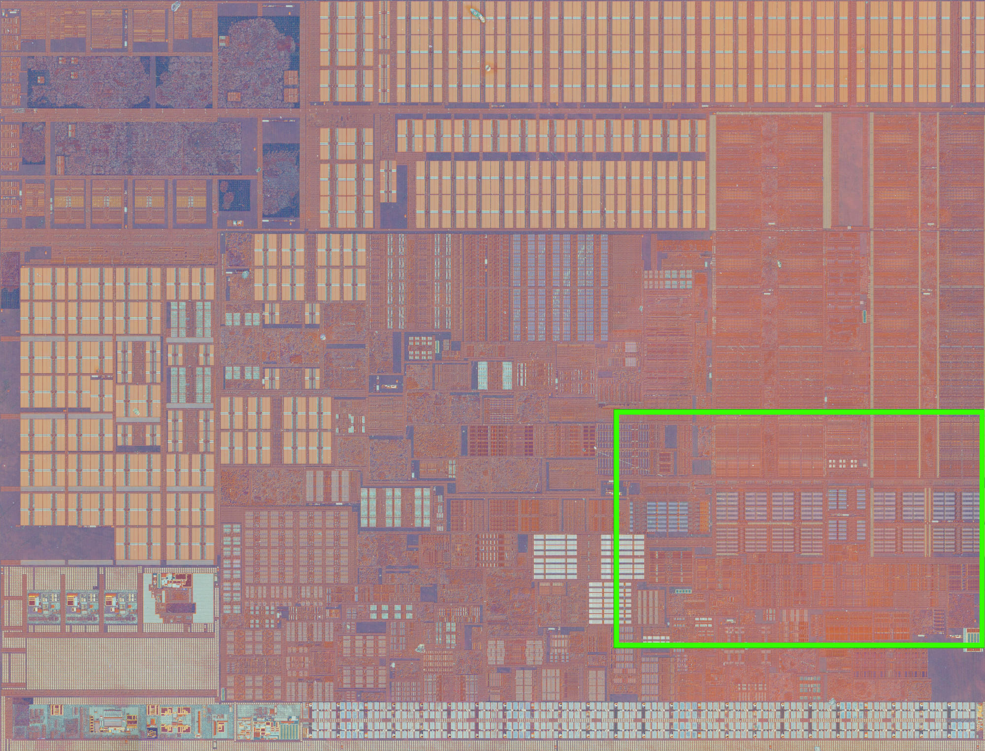
We’re interested in this die shot, recently released by Fritzchens Fritz on Flickr. We’ll be focusing on the highlighted area, which seems to have all the register files on the chip. If you want a full breakdown of the core, you can check guesses here on Twitter, on RWT and on Intel’s forums.
The Register Files
Here’s a close-up of that section, with the assumed register files and their purpose labeled2.
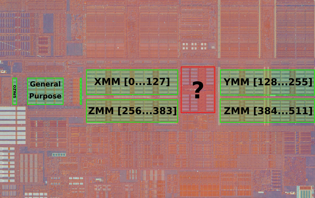
We guess the register file identities based on:
- The general purpose register files are of the right relative width (64 bits), and are in the right position below the integer execution units, and seem to have
EFLAGSnearby. - The SIMD registers are obvious from their size and positioning underneath the vector pipes.
- The upper 256 bits of the 512-bit
zmmregisters (labelled ZMM on the closeup) can be determined from comparing the SKL3 (no AVX-512) and SKX (has AVX-512) dies and noting that the bottom file is not present in SKL (a large empty area is present at that spot in SKL).
The Mystery Block
This leaves the mystery block in red. This block is in a prime spot below the vector execution units. Could it be the mask registers (kregs)? We found in the first post that the mask aren’t shared with either the scalar or SIMD registers, so we expect them to have their own physical register file. Maybe this is it?
Let’s compare the mystery register file to the integer register file, since they should be similar in size and appear to be implemented similarly:
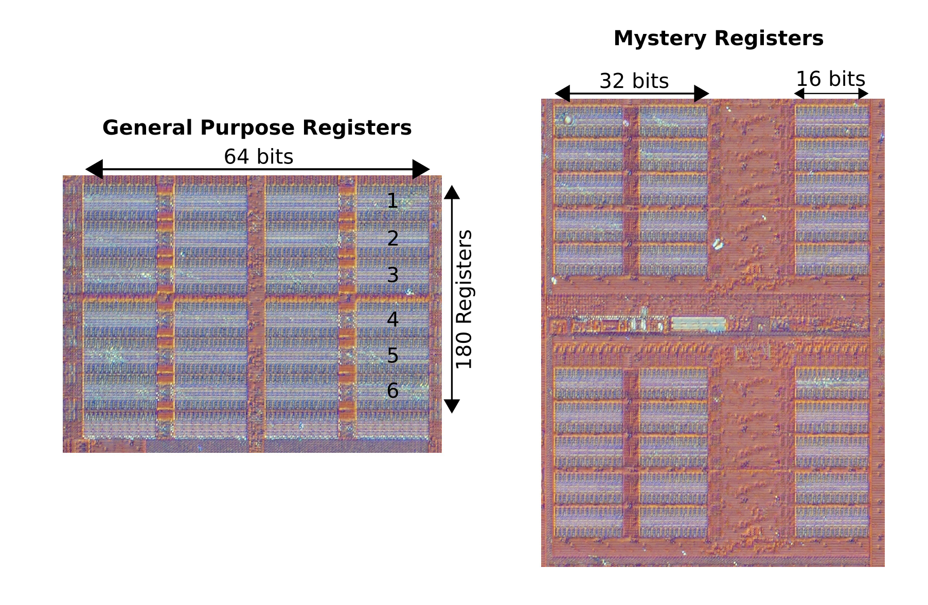
Looking at the general purpose register file on the left, each block (6 of which are numbered on the general purpose file) seems to implement 16 bits, as if you zoom in you see a repeating structure of 16 elements, and 4 blocks makes 64 bits total which is the expected width of the file. We know from published numbers that the integer register file has 180 entries, and since there are 6 rows of 4 blocks, we expect each row to implement 180 / 6 = 30 registers.
Now we turn our attention to the mystery file, with the idea that it may be the mask register file. There are a total of 30 blocks. Looking at the general purpose registers, we determined each block can hold 16 bits (horizontally) from 30 registers (vertically, I guess). So 30 blocks gives us: 30 blocks * 30 registers/block * 16 bits / 64 bits = 225 registers. It’s too much! We calculated last time that there are ~142 physical mask registers, so this is way too high.
There’s another problem: we only have three columns of 16-bit blocks, for a total of 48 bits, horizontally. However, we know that a mask register must hold up to 64 bits (when using a byte-wise mask for a full 512-bit vector register). Also, while our calculation above worked out to a whole number, the number of blocks (30) is not divisible by 4, so even if you assumed the arrangement of the blocks didn’t matter, there is no possible mapping from each register to 4 distinct blocks. Instead, we’d need something weird like 2 blocks providing 15 registers (instead of 30), but 64 bits wide (instead of 32). That seems very unlikely.
So let’s look just at the two paired columns on the left for now: a total of 20 blocks. If we take the SIMD registers as an example, it is not necessary that the full width of the register is present horizontally in a single row: the SIMD registers have only 256 bits in a row (split into two 128-bit lines), and then other other 256 bits in a 512-bit zmm register appear vertically below, in the register file marked ZMM in the diagram. So there’s a kind of over-under arrangement4.
Since the mask registers are associated with elements of the vector registers, maybe they are split up in the same way? That is, a 64-bit mask register uses one 2x16-bit (32-bit) chunk from the top half and one from the bottom half, to make up 64 bits? This is 20 total blocks, giving 150 registers by the same calculation above. This is much closer to the 142 we found by experiment.
Still… that nagging feeling. 142 is not equal to 150, and what about that third column of blocks? That doubt crept in: I had second thoughts that this was the mask register file after all. What could it be then?
Let’s Get Legacy
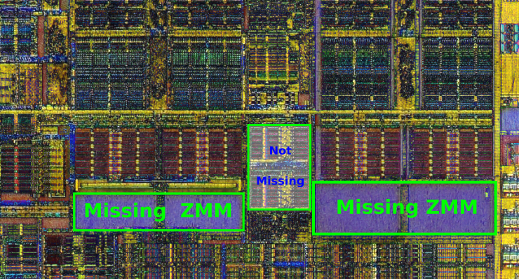
I realized there was one register file unaccounted for: the file for legacy x87 floating point and MMX. We expect that x87 floating point and MMX use the the same physical file because MMX registers are architecturally aliased onto the x87 registers5. So where is this file on the die? I looked all around6 the die shot. There are no good candidates.
So maybe this thing we’ve been looking at is actually the x87/MMX register file? In one way it’s a better fit: the x87 FP register file needs to be ~80 bits wide, so that would explain the extra column: if we assume each row is half of a register as before, that’s 96 bits. That’s enough to hold 80 bit extended precision values, and the 16 bits left over are probably could be used to store the FPU status word accessed by ftstw and related instructions. This status word is updated after every operation so must also be renamed for reasonable performance7.
Additional evidence that this might be the x87/MMX register file comes from this KBL die shot also from Fritz:
Note that while the high 256 bits of the register file are masked out (this chip supports only AVX2, not AVX-512 so there are no zmm registers), the register file we are considering is present in its entirety.
Cool theory bro, but aren’t we back to square zero? If this is the file for the x87/MMX registers, where do the mask registers live?
There’s one possibility we haven’t discussed although some of you might be screaming it at your monitors by now: maybe the x87/MMX and the kreg register files are shared. That is, physically aliased8 to the same register file, shared competitively.
Testing Our Theory
The good news? We can test for this, in software. That’s good, because I was never really that comfortable with this die shot thing and there was the risk that I would BS more than usual. Software-based uarch probing is a bit more my thing.
We’ll use the test method originally described by Henry Wong and which we used in the last post on this topic, and implemented in the robsize tool. Here’s the quick description of the technique, a straight copy/paste from that post:
We separate two cache miss load instructions by a variable number of filler instructions which vary based on the CPU resource we are > probing. When the number of filler instructions is small enough, the two cache misses execute in parallel and their latencies are overlapped so the > total execution time is roughly as long as a single miss.
However, once the number of filler instructions reaches a critical threshold, all of the targeted resource are consumed and instruction allocation > stalls before the second miss is issued and so the cache misses can no longer run in parallel. This causes the runtime to spike to about twice the > baseline cache miss latency.
Finally, we ensure that each filler instruction consumes exactly one of the resource we are interested in, so that the location of the spike indicates the size of the underlying resource. For example, regular GP instructions usually consume one physical register from the GP PRF so are a good choice to measure the size of that resource.
The trick we use to see if two register files are shared is first to use a test the size of each register file alone, using a test that uses filler that targets only that register file, then to run a third test whose filler alternates between instructions that use each register file. If the register files are shared, we expect all tests to produce the same results, since they are all drawing from the same pool. If the register files are not shared, the third (alternating) test should result in a much higher apparent resource limit, since two different pools are being drawn from and so it will take twice as many9 filler instructions to hit the RF limit.
Enough talk, let’s do this. I implemented several new tests in robsize to probe possible register sharing. First, we look at Test 38, which uses MMX instructions10 to target the size of the x87/MMX register file:

We see a clear spike at 128 instructions, so it seems like the size of the speculative11 x87/MMX register file is 128 entries.
Next, we have Test 43 which follows the same pattern as Test 38 but using kaddd as a filler instruction so targets the mask (kreg) register file:

This is mostly indistinguishable from the previous chart and we conclude that the size of the speculative mask register file is also 128.
Let’s see what happens when alternate MMX and another instruction type. Test 39 alternates MMX with integer SIMD instructions, and Test 40 alternatives with general purpose scalar instructions:


Both of these show the same effect: the effective resource limitation is much higher: around 210 filler instructions. This indicates strongly that the x87/MMX register is not shared with either the SIMD or scalar register files.
Finally, we get to the end of this tale, Test 41. This test mixes MMX and mask register instructions12:

This one is definitely not like the others. We see that the resource limit is now 128, same as for the single-type tests. We can immediately conclude that this means that mask registers and MMX registers are allocated from the same resource pool: they use the same physical register file.
This resolves the mystery of the missing register file: nothing is missing but rather this one register file simply serves double duty.
Normally a shared register file might be something to watch out for, performance-wise, but it is hard to imagine this having an impact in any non-artificial example. Who is going to be making heavy use of x87 or MMX (both obsolete) along with AVX-512 mask registers (the opposite end of the spectrum from “obsolete”)? It seems extremely unlikely. In any case, the register file is still quite large so hitting the limit is unlikely in any case.
So sharing these register files is a neat trick to reduce power and area: the register files aren’t all that big, but they live in pretty prime real-estate close to the execution units.
What’s cool about this one though is that is the first time that I’ve looked at a chip (that this is even possible is remarkable to me) and come up with a theory about the hardware we can test and confirm with a targeted microbenchmark. Here, it actually happened that way. I was already aware of the possibility of register file sharing (Henry had tests for this right in robsize from the start) – but although I considered other sharing scenarios I never considered sharing between x87/MMX and the mask registers until I tried to identify the register files on Franz’s die shots.
Some Missing Pieces
It seems like we’ve wrapped everything up nicely, but there are still a few rough edges.
- We calculated a total of 128 speculative registers, plus 16 non-speculative (to hold the 8 x87/MMX regs and the 8 kregs) is 144, but our ballpark estimate based on the regfile size was 150. Perhaps more importantly, with 5 rows of registers, we expect the number of registers to be a multiple of 5. Perhaps there are a handful of registers used from an unknown purpose or some other flaw in the test.
- I noticed an unexplained different in results between a test that uses a single instruction like
kaddd k1, k2, k3(test 27) and one that rotates through all the 8 registers:kaddd k0, k1, k1thenkaddd k1, k2, k2, etc (test 43). The former test results in an register file size of about 5 more than the latter. Similarly for tests using the MMX registers (compare tests 37 and 38). This post uses the rotate through all registers approach, while the original post used the fixed register variant in some cases so the number vary slightly. I have some theories but no definite explanation for this behavior.
Thanks
Thanks to Fritzchens Fritz who created the die shots analyzed here, and who graciously put them into the public domain.
Henry Wong who wrote the original article which introduced me to this technique and subsequently shared the code for his tool, which is now hosted on github.
Nemez who did a breakdown of the die shot, noting the register file in question as some type of integer register file, which originally piqued my curiosity.
Thanks to Daniel Lemire who provided access to the SKX hardware used in this post.
Thanks to Matt Godbolt and Vijay who pointed out typos in the text.
Discussion and Feedback
If you have something to say, leave a comment below or discuss this article on Hacker News.
Feedback is also warmly welcomed by email or as a GitHub issue.
-
Admittedly, “how many physical mask registers does the CPU have” is probably not a very high bar of interestingness to clear, to most people. ↩
-
The zmm, ymm and xmm registers all overlap, architecturally. That is,
xmm0is just the bottom 128 bits ofymm0, and similarly forymm0andzmm0. Physically, there are really onlyzmmregisters and the other two are simply specific ranges of bits of those larger register. So the area marked YMM on the die shot really means: the upper parts of theymmregisters which are not part of the corresponding xmm register. ↩ -
Actually Kaby Lake, since the best die shots we have are from that chip, but it’s the same thing. ↩
-
Incidentally, this lines up with an inspection of the execution units, which seem to have the same over-under arrangemnet: the port 5 FMA for example, looks like it has has two rows each with 4x 64-bit FMA units, rather than say a single row with 8 units. ↩
-
As a trick, I guess, to allow MMX registers to be saved and restored by operating systems and other code that weren’t aware of their presence. A similar mess occurred with the transition from SSE to AVX, where code unaware of AVX could accidentally clobber the upper part of AVX registers using SSE instructions (if SSE zeroed the upper bits), so instead we get the ongoing issue with legacy SSE and dirty uppers. ↩
-
This is a lie: I didn’t really look around all around the die: I looked near by the execution units were the register file would be with very high probability. ↩
-
The integer flags (so-called EFLAGS register) also need to be renamed and I believe they pull a similar trick: writing their results to the same physical register allocated for the result: I’ve marked the file that I think holds the so-called SPAZO group on the zoomed view, and the C flag may be stored in the same place or in the thin (single bit?) file immediately to the right of the GP file. ↩
-
I talk of physical aliasing here, to distinguish it from the logical/architectural aliasing. Logical aliasing is that which is visible to software: the
ymmandxmmregisters are logically aliased in that writes toxmm0show up in the low bits ofymm0. Similarly, the MMX and x87 register files are aliased in that writes to MMX register modify values in the FP register stack, although the rules are more complicated. Logical aliasing usually implies physical aliasing, but not the other way around. Physical aliasing, then, means that two register sets are renamed onto the same pool of physical registers, but this is usually invisible to software (except though careful performance tests, as we do here). ↩ -
In practice, you don’t actually get all the way to 2x: you hit something close to the ROB limit instead first. ↩
-
I use MMX rather than x87 so I don’t have to deal with the x87 FP stack abstraction and understand how that maps to renaming. ↩
-
The speculative register file because we expect some entries also to be used to hold the non-speculative values of the architectural registers. We’ll return to this point in a moment. ↩
-
Specifically, it mixes the same
kadddandporinstructions we used in the single-type tests Test 38 and Test 43. ↩
Comments
How big part of CPU is AVX512 ? is it possible to estimate that As when intel disabled AVX512 as consequence big little configuration I want to know how big part of silicon they just waste for this stupid decision :)
I have try the test 41, but it failed: Compiled Aug 29 2020 13:55:58 ibuf at 0x7f240c04e000 dbuf at 0x7f23fc04c000 Running test ID 41: alternating kaddd kN, kN+1, kN+1 and por mmN, mmN+1 Illegal instruction (core dumped)
my cpu is sandybridge 2600k.
Mask registers are a feature of AVX-512, an instruction set extension which isn’t available in Sandy Bridge. It is available starting in Skylake Xeon (SKX).
Unfortunately, this means you won’t be able to run this test (and several other tests in robsize which use AVX-512).
Seems like with simple Github Actions script, which automatically approves PRs with comments, this might be a nice solution for comments on Github pages!
What is “this”? The comment system on this blog? It is described over here.
If you want to automatically approve comments, that’s possible: it’s just a setting in staticman. I have the approval enabled as a form of moderation, but since I’ve gotten almost zero spam comments, I think maybe I could take that out and maybe let the comments be posted immediately.
Test comment. Just want to see how things look.